The Pseudo-Switch is
designed to bring together the convenience of fully solid-state electronics
with the practicality of mechanical multiple-throw switches. It includes a
push button and LED position indicators so that it can be used manually as
easily a regular switch, while also offering the fast response,
reliability, and versatility of a solid-state device.
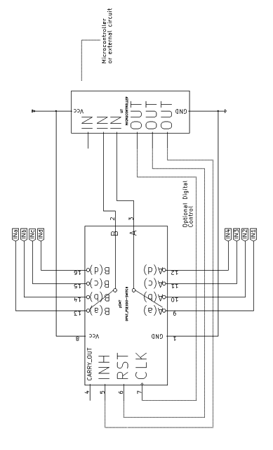
Digital control can also
be achieved via the Clock, Reset, and Inhibit inputs. These not only make
the difficulty of controlling analogue signals with digital circuitry a
breeze, but also allow multiple Pseudo-Switches to be combined for expanded
functionality. By exposing the Clock signal generated by the integrated
push button at the external Clock pin, the Pseudo-Switch makes it possible
for a microcontroller to both read in the switch position set by the user,
and advance that position automatically, using just one of its I/O pins.
This booklet will
demonstrate the basic, and advanced, circuit arrangements in which the
Pseudo-Switch can find use. Then finally, we'll look into the
internals to find out what makes it tick.
|
Supply Voltage
|
3.0 - 5.5V DC
|
|
Supply Current
|
<50mA
|
|
Max. Input Voltage
|
+5.0V, -4.5V(3V Vcc) +5.5V, -5.5V(5V Vcc)
|
|
Max. Switch Current
|
20mA
|
|
Switch ON Resistance
|
<120 - 500 Ohms
|
|
Switching Time
|
2 Microseconds
|
|
Switching Configuration
|
Break Before Make
|
|
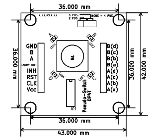
Dimensions
|
43x42mm
|
Table
1, Specifications.
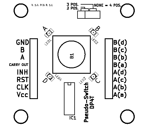
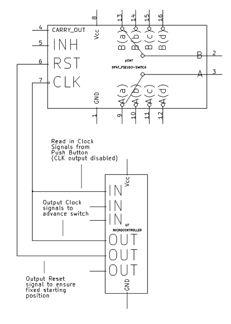
The pin functions are
conveniently described on the top silkscreen of the Pseudo-Switch circuit
board:
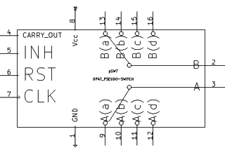
The switch connections
are alphabetically labeled, so that the pole of the first switch (A) is
switched between connections Aa, Ab, Ac, and Ad. Similarly, the second
switch (B) joins with Ba, Bb, Bc, and Bd. This can be seen more clearly
using the following functional diagram.
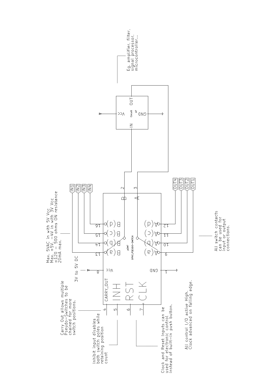
The other pins are for
digital control of the Pseudo-Switch and may all be left open-circuit if
only manual control using the built-in push button is required. Their
functions are as follows:
·
Clock Switch position advances when this
signal transitions from High to Low. Normally pulled High via 330Kohm
resistance, it is pulled Low via 16Kohms when the built-in push button is
pressed and this can be detected externally if connected to a digital
input. It can be connected to a digital output for external control.
·
Reset When brought High, this resets the
switch at position "A". This is helpful for making sure that the
switch is at a known position before advancing it digitally. It is pulled
Low internally via 56Kohms.
·
Inhibit When brought High, this
disconnects all the switch contacts regardless of which is selected. The
previously selected contact is connected again when the signal is brought
back Low. This is handy for multiplexing signals from many Pseudo-Switches
into one input or output. It is pulled Low internally via 330Kohms.
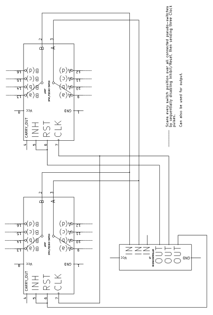
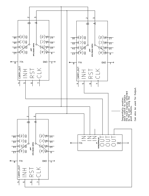
·
Carry Out When the end of the position
range is reached, this line is pulsed before the switch resets to position
"A". This can be used to connect with the Clock input of a
further Pseudo-Switch to allow them to be combined for a larger number of
effective switch positions.
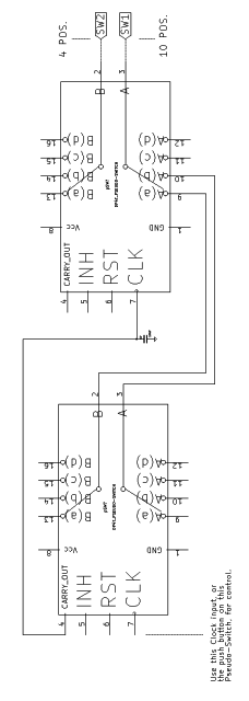
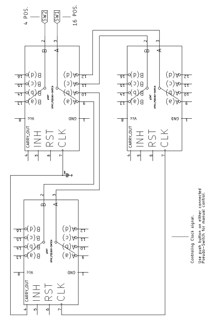
The
number of positions which the switch covers before resetting back to
position "A" is set using the jumper at the top of the board, as
described on the top silkscreen.
The last two positions
will take four Clock pulses to advance over.
Alternatively, limit the
second Pseudo-Switch to two positions for a total of eight.
This
is an example C function to advance the position of the switch a specified
number of places, optionally resetting it beforehand to ensure the final
position is correct regardless of whether the built-in push button has been
pressed to advance the position manually. It also sets the state of the
Inhibit function.
Fill
in the missing definitions to suit your microcontroller configuration.
//
Example Configuration function for Pseudo-Switch Analogue Switch Board from
OmberTech
// 2018 OmberTech. No warranty. May be used
for any purpose.
#define
MICROSECOND // Approximate number of execution cycles
required for CPU to complete "for" loop in microsleep function.
// Microcontroller outputs connected to
Pseudo-Switch:
#define CLOCK
#define RESET
#define INHIBIT
//
Delay for specified number of microseconds (alternatively use hardware
timer):
void microsleep (unsigned int microseconds)
{
unsigned long i;
while (microseconds--)
for ( i = 0 ; i < MICROSECOND ; i++
);
}
// Modify Pseudo-Switch configuration:
void
pseudosw ( unsigned int clk, // Number of switch positions to be advanced
char rst, // If 1, reset switch position to "A" before
advancing position
char inh ) // If 1, enable Inhibit mode (no switch contacts
selected). If 0, disable Inhibit mode.
{
INHIBIT = inh;
if (rst)
{
RESET = 1;
RESET = 0;
microsleep (5);//Ensure Reset has been disabled
}
for ( ; clk > 0 ; clk-- )
{
CLOCK = 1;
CLOCK = 0;
}
microsleep (5); // Wait for switching time
}
The
above code can be downloaded in text format, and without the wrapped
comments, from:
http://www.computernerdkev.heliohost.org/pseudoswitch/
Using
the above function, this would move the switch to the fourth position (D):
pseudosw
(3,1,0);
While
this would advance it two positions ahead of its previous position (the
switch will loop back around if it reaches the last position):
pseudosw (2,0,0);
Finally,
this turns on the Inhibit function of the Pseudo-Switch without changing
its set position:
pseudosw (0,0,1);
Which
is actually equivalent to:
INHIBIT = 1;
The Pseudo-Switch board
can be mounted to an instrument case using 3mm or 1/8 inch bolts and
suitable spacers. If manual control is desired, a suitable hole should be
placed to allow both access to the push button, and to leave the position
indicator LEDs visible.
Dimensions
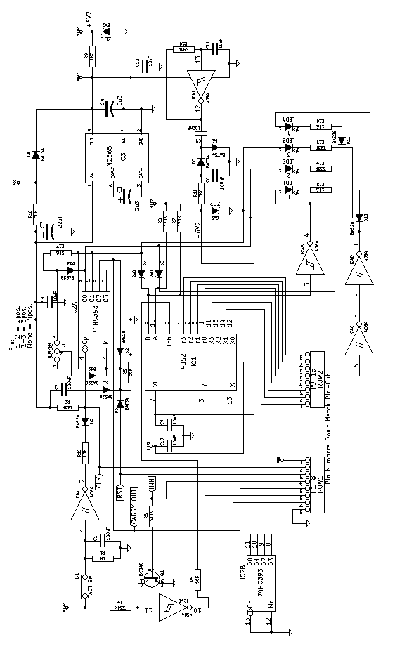
The
following schematic describes the circuitry that drives the Pseudo-Switch.
To facilitate switching 5V signals from 3V circuits, and to allow negative
voltages and AC signals, a voltage doubler and a voltage inverter are
included. In total four internal power lines are used, along with Ground:
Vcc (3V - 5V DC), VinX2 (the doubled output voltage from IC3), +6.2V, and
-6.2V. Additionally, Vcc is supplied via a 30 ohm resistor to all
connections except D4 in order to protect IC3, as described later.
CAD
generated and hand drawn copies of the schematic are shown on the following
pages.
Signal
Control:
The
switching of "switch positions" is achieved electronically using
a 4052 analogue switch IC, controlled by the binary counter IC2A (74HC393)
at pins 9 and 10 (inputs A and B). in addition the Inhibit input, pin 6, is
controlled externally via IC4E and Q1 which together form a non-inverting
buffer that also performs the required logic level conversion from the
input voltage up to that of the internal 6.2V supply. R6 limits the current
that may flow from IC4E to ZD1 via IC1's input protection diode when
the supply voltage to IC4 is above that of the regulated 6.2V line powering
IC1.
IC1
is conveniently designed to reference GND for its control inputs, with a
separate connection for negative voltage to use with its internal analogue
switching circuitry. This avoids the need for negative voltages to be
supplied to the control inputs when they are brought Low.
The
binary counter IC2A is powered from Vcc, and advances on the High to Low
transition of its Clock input, pin 1. This pin is normally held High by R2
when not pulled down by an external circuit connection. When B1 is pressed,
the input to IC4A (4584 Schmitt Inverter) is brought High, once de-bouncing
capacitor C1 is charged. This produces a low output that pulls down the
Clock input of IC2A via R12 (which prevents damage to an external circuit
which may override the signal) and advances the switch position count. D9
prevents the boosted voltage of IC4's High output from being applied
to IC2 or an external circuit.
IC2A's
Reset input, pin 2, is pulled Low via R3 except for when one of the four
diodes connected to it force it High. When the position jumper, J1, is in
the "2pos." setting, this happens after the count advances to
position 2 and IC2 pin 4 goes High. In the "3pos." setting, it is
when both pin 3 and pin 4 are High. If neither of these positions are
selected, D2 ensures a default maximum position by resetting the counter at
position 4, which is when pin 5 goes High. D1 resets the counter when power
is first applied, and D3 allows external reset control.
The
LEDs showing the current switch position are arranged so that sufficient
voltage to light them is only available when the output combination
corresponding with their indicated position is at IC2A's outputs.
Three more inverters from IC4 are used to achieve this. In order to drive
the inputs to these inverters, and to IC1, 2V zener diodes D7 and D8, along
with pull-up resistors R7 and R8, increase the High level voltage above the
output of IC2A while ensuring that the Low voltage is still below the input
threshold.
Power
Supply
A
positive and negative internal supply above the Vcc level is required to
allow the switching of AC signals and to permit reverse current flow in
analogue circuits at voltages that may be above the input supply. The first
stage is IC3 (LM2665), which is a dedicated voltage doubler IC from Texas
Instruments using the switched capacitor method. Internally it uses CMOS
analogue switches to charge capacitor C3, then add the voltage over it to
the charge of C4 at the output. The LM2665 actually takes the voltage
supply for its own internal circuitry from the output. As a result, D4 is
required in order for it to start when power is first applied.
Because
CMOS inputs can be damaged if they are at a higher voltage than the supply,
an issue is found if the voltage drop over D4 and the charge time of C4
results in the "V+" input being higher than the output at
start-up. To avoid this, R18 limits the rate at which the supply voltage
rises as it charges filter capacitor C7, while D4 connects directly to the
input supply to make sure that C4 reaches full charge before this. D4 is
also a schottky type diode, with a lower forward voltage than silicon types.
The
output of the voltage doubler is regulated to 6.2V by ZD1 to power IC1
(4052) and other discrete circuit components. However the supply to IC4
(4584) taps in before this in order to receive the maximum voltage and
current to power the negative voltage generator built with IC4F.
As a
schmitt inverter, IC4F is able to be turned into an oscillator by simply
adding a capacitor on its input with a resistor connecting it to the
output. The resulting square wave, at roughly 160KHz frequency, is applied
to C5. This forms the beginning of a conventional negative voltage
generator circuit which is built using schottky diodes for minimum voltage
drop. The output is regulated to -6.2V by ZD2 and connects with the VEE
input of IC1 (4052).