

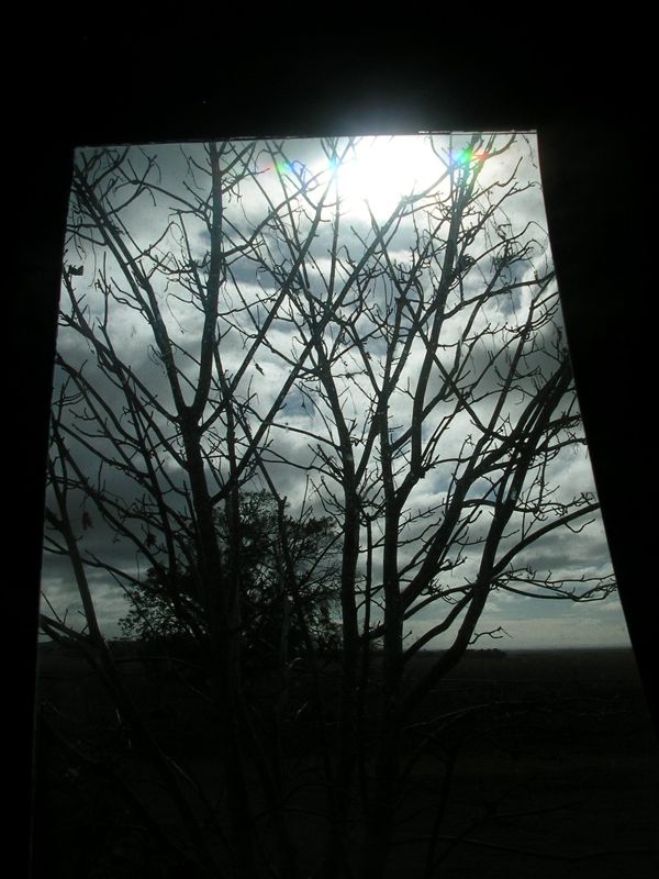
The effect is slightly less visible to a camera, though it can also offer a more subtle effect in darker scenes that may be useful for photography.
Computer Nerd Kev |
Home|About|Projects|Links |
Projects > Rainbow Glasses |
LCD Shutterglasses Rainbow Adapter |
While experimenting with LCD shutterglasses for active 3D TVs and PC adapters, I happened across a state in which the LCDs begin to exhibit a refractive effect that surrounds reflective objects viewed through them with a rainbow coloured halo.
The effect is slightly less visible to a camera, though it can also offer a more subtle effect in darker scenes that may be useful for photography.
While sensitive to voltage and frequency, the effect presented itself in two different models of active 3D shutterglasses produced more than a decade apart (though a later test with another model failed to work, so compatibility does vary). The trick is to slowly discharge the capacitive LCD "lenses" during one stage within an otherwise normal drive pattern. The overall drive signal applied over each "lens" is shown below.
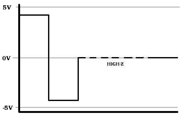
Drive signal to one LCD element with Ground measured from LCD Common.
The device that I designed to drive the glasses is available for sale as a kit, or pre-assembled, at the OmberTech online store. Or at Tindie.
Please let me know the results for other models. Email:
3/4/2022
Tests with beams from red laser diodes (three used in the photos below) reveal a pattern that suggests the LCD may be acting as a diffraction grating.
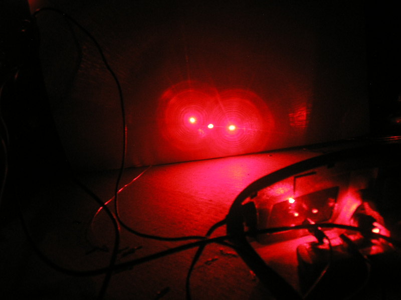
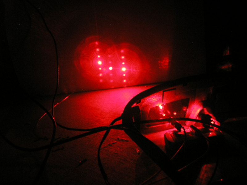
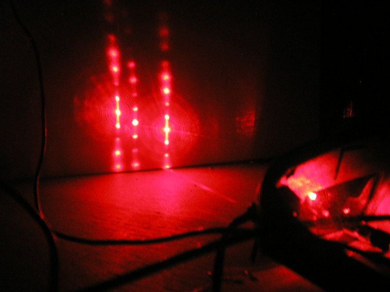
Showing left to right: circuit off, circuit on, and boost on.
The left and right lasers have a more focused beam than the middle one, causing a greater effect.
The following is from the OmberTech booklet, which can be downloaded above.
The "lenses" in the LCD Shutterglasses are equivalent to single pixels in a monochrome Liquid Crystal Display, or single elements of a 7-segment numeric display. The "D" in "LCD Shutterglasses" is therefore out of place because there is nothing that can really be displayed by glasses with lenses that in normal use can only be transparent or opaque.
From an electrical perspective the elements themselves act as capacitors. When charged, the Liquid Crystal molecules align to straighten out a twist in their structure that otherwise rotates the polarisation of light passing through. By placing polarising filters either side of the crystals, when the polarisation of the light is opposite to the outer filter, no light can get through at all. Depending on the filter this can happen in either the charged or discharged state of the LCD element. Most commonly it is in the charged state, so when a signal is applied the element becomes opaque.
It would seem that this signal might simply be a fixed voltage difference, but to complicate matters LCD elements perform best and live longest when the polarity of their charge is constantly changed. The signal therefore needs to be rapidly alternating from High to Low in opposite states across the LCD element's two electrical connections. Then it appears opaque until the element is shorted so that it can allow light to pass through once more.
In this circuit we add one more input state for this capacitive LCD element, which discharges it slowly so that it fades out rather than being shorted out and made immediately transparent. A possible explanation for the resulting effect is that the slow discharge results in the liquid crystal molecules lingering in a partially twisted state, thereby partially rotating the polarisation of the light passing through. The wavelength of the light influences the degree of rotation that takes place, so the different colours of light become visible in bands, as in a rainbow.
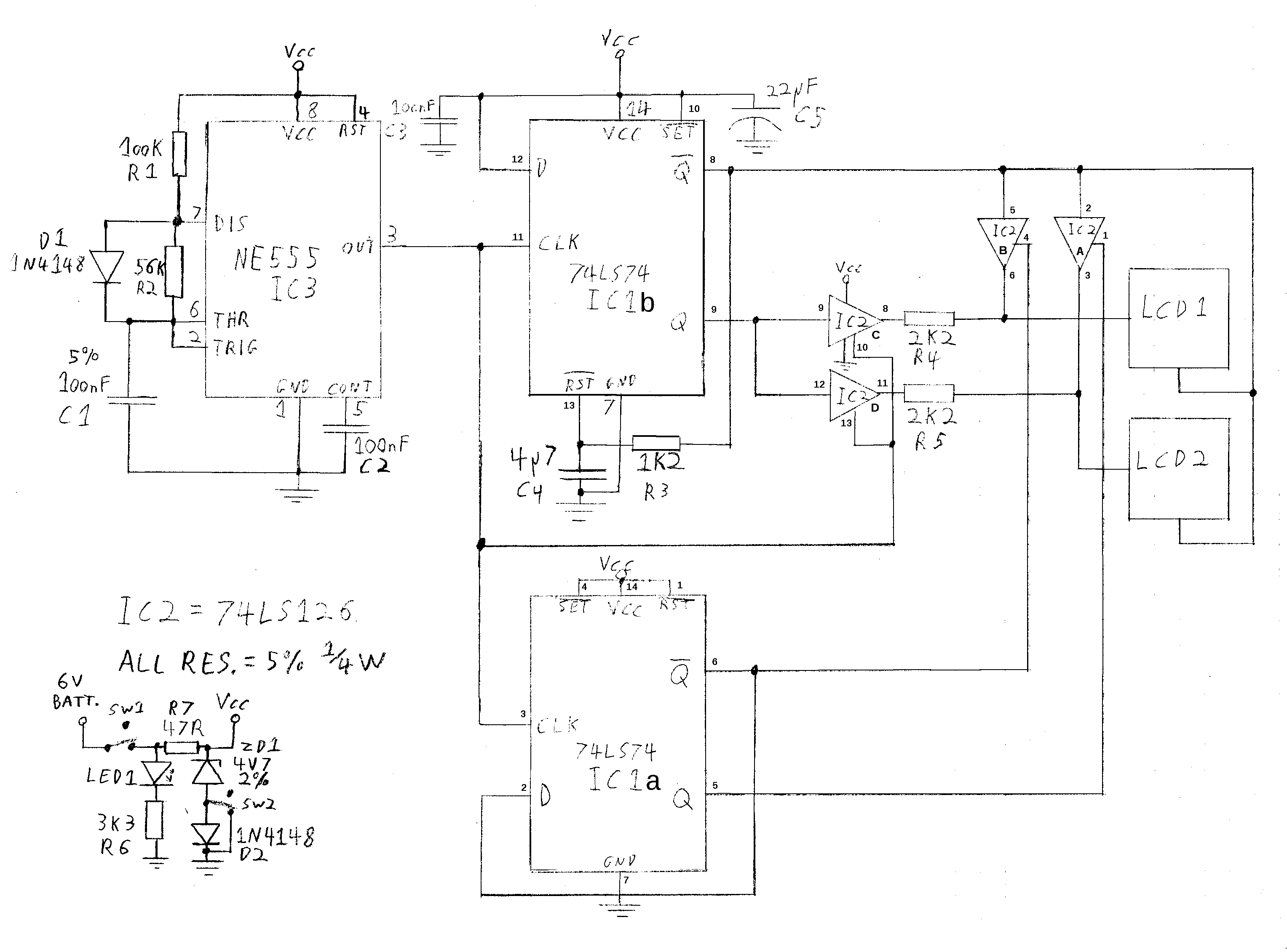
Adapter Schematic
IC3 is that old favourite the 555 timer, here configured with D1 ensuring a longer On time than Off time by allowing C1 to bypass R2 when it charges while the output is High.
At the same time as this output is High, IC2c/d (74LS126) are enabled, allowing the non-inverted output of the IC1b (74LS74) Flip-Flop to be applied to R4 and R5. When the clock signal from IC3 goes from Low to High, the Flip-Flop output likewise goes Low to High as well. But at the same time C4 begins to discharge via R3, connected to the Flip-Flop's inverted output, and eventually causes it to reset, bringing the non-inverted output back Low again.
This oscillation alternately charges the active LCD element because the opposite states of the inverted and non-inverted Flip-Flop outputs are applied to it.
Meanwhile, the inactive element is shorted out by either IC2a or IC2b. These force both of the LCD connections to an equal voltage and thereby discharge its capacitance. The active element is alternated on each clock cycle by Flip-Flop IC1a which toggles the Enable inputs of the IC2a/b 3-state buffers.
The connection of the Enable inputs of the other 3-State buffers IC2c/d to the clock signal allows the active LCD element to be discharged slowly for the Low period of the clock waveform (set by R2) when all the buffers on one of its connections are in 3-State mode. This fades out from the charged, opaque, state that it was in during the preceeding High period of the clock waveform.
Finally, the effect was found only to work at drive lower voltages to the LCD elements, but with an increased brilliance when the circuit supply voltage was quickly raised from around 4.75V to above 5V, before fading out. The power regulation part of the circuit, shown in the bottom left of the schematic, makes sure that the normal supply voltage is set for optimal performance by using ZD1 to keep it within 2% of 4.7V. SW2 effectively switches a silicon diode in series with ZD1's path to GND, increasing the voltage across it, and therefore the circuit supply voltage, by at most about 0.7V. This provides the "Boost" functionality, but unfortunately also introduced circuit instability with some 74LS74 ICs. The power LED is connected to the unregulated part of the supply to prevent unneeded power dissipation across R7.